(China (Mainland))

Product Summary
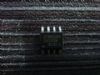
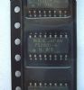
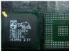
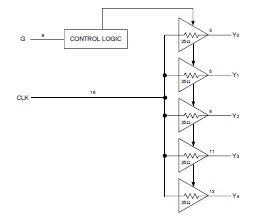
The IDT5V2305PGI is a high performance, low skew clock buffer that operates up to 200MHz. One bank of five outputs provides low skew copies of CLK. Through the use of control pin G, the outputs of bank Y(0:4) can be placed in a low state regardless of CLK input. The IDT5V2305PGI operates in 2.5V and 3.3V environments. The built-in output enable glitch suppression ensures a synchronized output enable sequence to distribute full period clock signals. The IDT5V2305PGI is characterized for operation from -40℃ to +85℃.
Parametrics
IDT5V2305PGI absolute maximum ratings: (1)VDD Power Supply Voltage: –0.5 to +4.6 V; (2)VI Input Voltage: –0.5 to VDD +0.5 V; (3)VO Output Voltage: –0.5 to VDD +0.5 V; (4)IIK Input Clamp Current VI < 0 or VI > VDD: ±50 mA; (5)IOK Output Clamp Current VO < 0 or VO > VDD: ±50 mA; (6)IO Continuous Total Output Current VO < 0 to VDD: ±50 mA; (7)TSTG Storage Temperature: –65 to +150 ℃.
Features
IDT5V2305PGI features: (1)High performance 1:5 clock driver for general purpose applications; (2)Operates up to 170MHz at VDD = 2.5V; (3)Operates up to 200MHz at VDD = 3.3V; (4)Pin-to-pin skew < 50ps; (5)VDD range: 2.3V to 3.6V; (6)Output enable glitch suppression; (7)25Ω on-chip series dampening resistors; (8)Available in TSSOP and VFQFPN packages.
Diagrams
| Image | Part No | Mfg | Description |  |
Pricing (USD) |
Quantity | ||||
|---|---|---|---|---|---|---|---|---|---|---|
 |
 IDT5V2305PGI |
|
IC CLK BUFFER 1:5 200MHZ 16TSSOP |
Data Sheet |
Negotiable |
|
||||
|
IDT5V2305PGI8 |
|
IC CLK BUFFER 1:5 200MHZ 16TSSOP |
Data Sheet |
Negotiable |
|
||||