(China (Mainland))


Product Summary
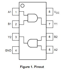
The NL27WZ08US is a high performance dual 2–input AND Gate operating from a 1.65 V to 5.5 V supply.
Parametrics
NL27WZ08US absolute maximum ratings: (1)VCC, DC Supply Voltage: -0.5 to 7.0 V; (2)VI, DC Input Voltage: -0.5 to 7.0 V; (3)VO, DC Output Voltage: -0.5 to VCC + 0.5 V; (4)IIK, DC Input Diode Current VI < GND: -50 mA; (5)IOK, DC Output Diode Current VO < GND: -50 mA; (6)IO, DC Output Sink Current: ±50 mA; (7)ICC, DC Supply Current per Supply Pin: ±100 mA; (8)IGND, DC Ground Current per Ground Pin: ±100 mA; (9)TSTG, Storage Temperature Range: -65 to 150℃; (10)TL, Lead Temperature, 1 mm from Case for 10 Seconds: 260℃; (11)TJ, Junction Temperature under Bias: 150℃; (12)θJA, Thermal Resistance: 250℃/W; (13)PD, Power Dissipation in Still Air at 85℃: 250 mW; (14)MSL, Moisture Sensitivity: Level 1; (15)FR, Flammability Rating Oxygen Index: 28 to 34 UL 94 V–0 @ 0.125 in; (16)VESD, ESD Withstand Voltage Human Body Model: 2000V; (17)ILatch–Up, Latch–Up Performance Above VCC and Below GND at 85℃: ±500 mA.
Features
NL27WZ08US features: (1)Extremely High Speed: tPD 2.5 ns (typical) at VCC = 5 V; (2)Designed for 1.65 V to 5.5 V VCC Operation; (3)Over Voltage Tolerant Inputs; (4)LVTTL Compatible – Interface Capability With 5 V TTL Logic with VCC = 3 V; (5)LVCMOS Compatible; (6)24 mA Balanced Output Sink and Source Capability; (7)Near Zero Static Supply Current Substantially Reduces System Power Requirements; (8)Replacement for NC7WZ08; (9)Chip Complexity: FET = 124.
Diagrams
| Image | Part No | Mfg | Description |  |
Pricing (USD) |
Quantity | ||||||||||||
|---|---|---|---|---|---|---|---|---|---|---|---|---|---|---|---|---|---|---|
 |
 NL27WZ08US |
|
IC GATE AND DUAL 2INPUT HP US8 |
Data Sheet |
Negotiable |
|
||||||||||||
 |
NL27WZ08USG |
ON Semiconductor |
Gates (AND / NAND / OR / NOR) 1.65-5.5V Dual 2-Input AND |
Data Sheet |
|
|
||||||||||||