(China (Mainland))

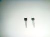
Product Summary
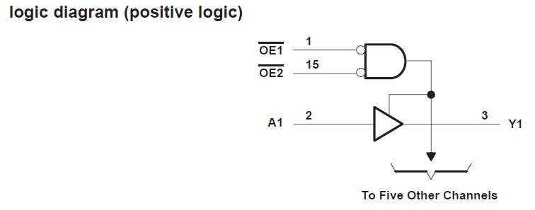
The SN74HC365DR is a hex buffer and line driver. It is designed specifically to improve both the performance and density of 3-state memory address drivers, clock drivers, and bus-oriented receivers and transmitters. The SN74HC365DR contains six independent buffers/drivers with dual-gated output-enable (OE1 and OE2) inputs. When OE1 and OE2 are both low, the SN74HC365DR passes noninverted data from the A inputs to the Y outputs. If either (or both) output-enable terminal(s) is high, the outputs are in the high-impedance state.
Parametrics
SN74HC365DR absolute maximum ratings: (1)Supply voltage range, VCC: -0.5 V to 7 V; (2)Input clamp current, IIK (VI < 0 or VI > VCC): ±20 mA; (3)Output clamp current, IOK (VO < 0 or VO > VCC): ±20 mA; (4)Continuous output current, IO (VO = 0 to VCC): ±35 mA; (5)Continuous current through VCC or GND: ±70 mA; (6)Package thermal impedance, θJA: D package: 73℃/W, N package: 67℃/W, NS package: 64℃/W, PW package: 108℃/W; (7)Storage temperature range, Tstg: -65℃ to 150℃.
Features
SN74HC365DR features: (1)Wide Operating Voltage Range of 2 V to 6 V; (2)High-Current 3-State True Outputs Can Drive Up To 15 LSTTL Loads; (3)Low Power Consumption, 80-μA Max ICC; (4)Typical tpd = 13 ns; (5)±6-mA Output Drive at 5 V; (6)Low Input Current of 1 μA Max.
Diagrams
| Image | Part No | Mfg | Description |  |
Pricing (USD) |
Quantity | ||||||||||||
|---|---|---|---|---|---|---|---|---|---|---|---|---|---|---|---|---|---|---|
 |
 SN74HC365DR |
Texas Instruments |
Buffers & Line Drivers Hex Buff & Line Drv w/3-State Outputs |
Data Sheet |
|
|
||||||||||||
|
SN74HC365DRE4 |
Texas Instruments |
Buffers & Line Drivers Hex Buff & Line Drv w/3-State Outputs |
Data Sheet |
|
|
||||||||||||
|
SN74HC365DRG4 |
Texas Instruments |
Buffers & Line Drivers Hex Buffers And Line Drivers |
Data Sheet |
|
|
||||||||||||