(China (Mainland))

Product Summary
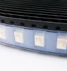
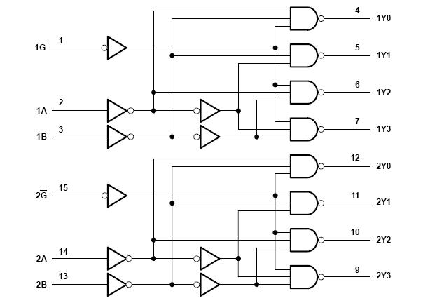
The SN74LV139ADBR is a dual 2-line to 4 line decoder/demultiplexer. It is designed for 2-V to 5.5-V VCC operation. The SN74LV139ADBR is designed for high-performance memory-decoding or data-routing applications requiring very short propagation delay times. In high-performance memory systems, these decoders can minimize the effects of system decoding. When employed with high-speed memories utilizing a fast enable circuit, the delay time of these decoders and the enable time of the memory usually are less than the typical access time of the memory. This means that the effective system delay introduced by the decoders is negligible. The SN74LV139ADBR comprises two individual 2-line to 4-line decoders in a single package. The active-low enable (G) input can be used as a data line in demultiplexing applications. It features fully buffered inputs, each of which represents only one normalized load to its driving circuit.
Parametrics
SN74LV139ADBR absolute maximum ratings: (1)Supply voltage range, VCC:–0.5V to 7V; (2)Input voltage range, VI:–0.5V to 7V; (3)Voltage range applied to any output in the high-impedance; (4)or power-off state, VO:–0.5V to 7V; (5)Output voltage range, VO:–0.5V to VCC + 0.5V; (6)Input clamp current, IIK (VI<0):–20mA; (7)Output clamp current, IOK (VO<0 or VO>VCC): ±50mA; (8)Continuous output current, IO (VO = 0 to VCC): ±25mA; (9)Continuous current through VCC or GND: ±50mA; (10)Package thermal impedance, θJA: 82°C/W; (11) Storage temperature range, Tstg:–65°C to 150°C.
Features
SN74LV139ADBR features: (1)2-V to 5.5-V VCC Operation; (2)Max tpd of 7.5 ns at 5V; (3)Support Mixed-Mode Voltage Operation on All Ports; (4)Designed Specifically for High-Speed Memory Decoders and Data-Transmission Systems; (5)Incorporate Two Enable Inputs to Simplify Cascading and/or Data Reception; (6)Ioff Supports Partial-Power-Down Mode Operation; (7)Latch-Up Performance Exceeds 250mA Per JESD 17; (8)ESD Protection Exceeds JESD 22: 2000-V Human-Body Model (A114-A), 200-V Machine Model (A115-A), 1000-V Charged-Device Model (C101).
Diagrams
| Image | Part No | Mfg | Description |  |
Pricing (USD) |
Quantity | ||||||||||||
|---|---|---|---|---|---|---|---|---|---|---|---|---|---|---|---|---|---|---|
 |
 SN74LV139ADBR |
Texas Instruments |
Encoders, Decoders, Multiplexers & Demultiplexers Dual |
Data Sheet |
|
|
||||||||||||
|
SN74LV139ADBRE4 |
Texas Instruments |
Encoders, Decoders, Multiplexers & Demultiplexers Dual 2 to 4-Line Decdr/Demltplxer |
Data Sheet |
|
|
||||||||||||
|
SN74LV139ADBRG4 |
Texas Instruments |
Encoders, Decoders, Multiplexers & Demultiplexers Dual 2Line To 4Line Decodr Demultiplexer |
Data Sheet |
|
|
||||||||||||