(China (Mainland))

Product Summary
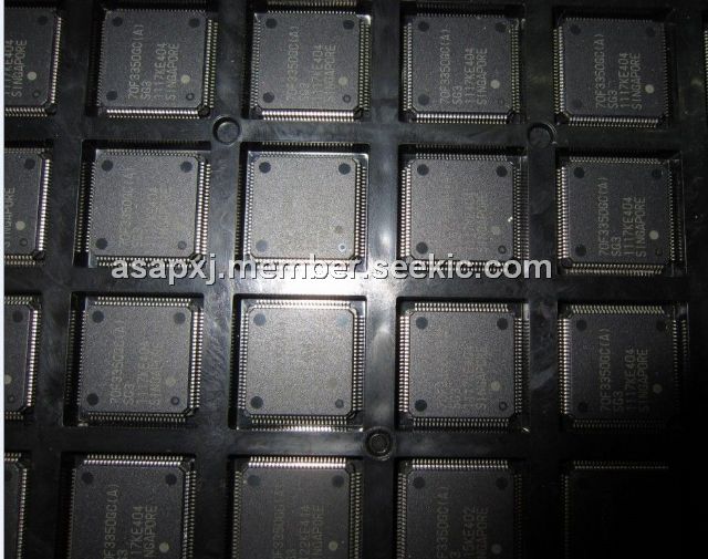
The UPD70F3350GC(A) is a 32-bit V850ES RISC 512KB Flash.
Parametrics
UPD70F3350GC(A) absolute maximum ratings: (1)Package: 100LQFP ; (2)Family Name: V850ES ; (3)Program Memory Type: Flash ; (4)Program Memory Size: 512 KB ; (5)Maximum Speed: 32 MHz ; (6)Data Bus Width: 32 Bit ; (7)RAM Size: 40 KB ; (8)Operating Supply Voltage: 3.3 V ; (9)Operating Temperature: -40℃ to 85℃; (10)Interface Type: CAN/CSI/I2C/UART ; (11)On-Chip ADC: 12-chx10-bit ; (12)On-Chip DAC: 2-chx8-bit ; (13)Number of Programmable I/Os: 84 ; (14)Number of Timers: 8.
Features
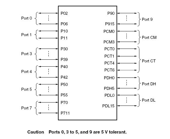
UPD70F3350GC(A) features: (1) Minimum instruction execution time: 31.25 ns (operating with main clock (fXX) of 32 MHz); (2)General-purpose registers: 32 bits×32 registers; (3)CPU features: Signed multiplication (16×16 → 32): 1 to 2 clocks, Signed multiplication (32×32 → 64): 1 to 5 clocks, Saturated operations (overflow and underflow detection functions included), 32-bit shift instruction: 1 clock, Bit manipulation instructions, Load/store instructions with long/short format; (4)Memory space: 64 MB of linear address space (for programs and data), External expansion: Up to 4 MB; (5)Interrupts and exceptions: Non-maskable interrupts: 2 sources, Maskable interrupts: 59 sources, Software exceptions: 32 sources, Exception trap: 2 sources; (6)I/O lines: I/O ports: 84; (7)Timer function: 16-bit interval timer M (TMM): 1 channel, 16-bit timer/event counter P (TMP): 6 channels, 16-bit timer/event counter Q (TMQ): 1 channel, Watch timer: 1 channel, Watchdog timer: 1 channel; (8)Real-time output port: 6 bits ×1 channel; (9)Serial interface: Asynchronous serial interface A (UARTA), 3-wire variable-length serial interface B (CSIB), I2C bus interface (I2C), UARTA/CSIB: 1 channel, UARTA/I2C: 2 channels,; (10)CSIB/I2C: 1 channel, CSIB: 3 channels; (11)IEBus controller: 1 channel; (12)CAN controller: 1 channel (CAN controller versions only); (13)A/D converter: 10-bit resolution: 12 channels; (14)D/A converter: 8-bit resolution: 2 channels; (15)DMA controller: 4 channels; (16)CRC function: 16-bit error detection codes are generated for data in 8-bit units; (17)Debug control unit (DCU): JTAG interface; (18)ROM correction: 4 correction addresses specifiable; (19)Clock generator: During main clock or subclock operation; (20)7-level CPU clock (fXX, fXX/2, fXX/4, fXX/8, fXX/16, fXX/32, fXT); (21)Clock-through mode/PLL mode selectable; (22)Internal oscillation clock: 220 kHz (TYP.); (23)Power-save functions: HALT/IDLE1/IDLE2/STOP/subclock/sub-IDLE Package: 100-pin plastic LQFP (fine pitch) (14×14).
Diagrams
 |
 UPD70008AG-4 |
Other |
|
Data Sheet |
Negotiable |
|
||||
|
UPD70236AGD-10-5BB |
Other |
|
Data Sheet |
Negotiable |
|
||||
|
UPD7030025AGC-25 |
Other |
|
Data Sheet |
Negotiable |
|
||||
|
UPD703014A |
Other |
|
Data Sheet |
Negotiable |
|
||||
|
UPD703014AY |
Other |
|
Data Sheet |
Negotiable |
|
||||
|
UPD703015A |
Other |
|
Data Sheet |
Negotiable |
|
||||